| Tutorial >> The ONL Architecture |
|
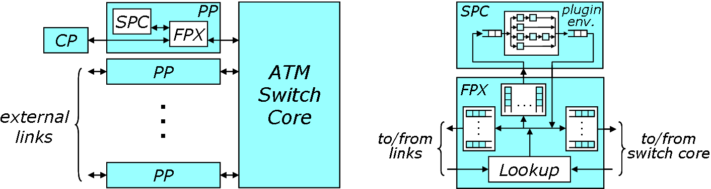
Washington University's gigabit router architecture is designed to be a scalable, high-performance, open platform for conducting network research. It employs highly reconfigurable technology (programmable hardware and dynamic software modules) to provide high-speed processing of both IP packets (with and without active processing) and ATM cells. Fig. 1 shows the overall architecture of the NSP and its main components: Control Processor (CP), ATM switch core, Field Programmable port eXtenders (FPXs), Smart PortCards (SPCs) and Line Cards (LCs).
The main function of the router is to forward packets at a high speed from its input side to its output side. The system uses a multistage interconnection network with dynamic routing and a small internal speed advantage (i.e., the internal data paths can forward packets at a faster rate than the external links) to connect the Input side Port Processors (IPPs) to the Output side PPs (OPPs). A PP can be either a Field Programmable port eXtender (FPX) and/or a Smart PortCard (SPC). An FPX is a reprogrammable hardware device, and an SPC is a general-purpose processor. These PPs perform packet classification, route lookup and packet scheduling. In this tutorial, we will assume a full configuration in which each PP consists of an FPX-SPC combination.
Data packets enter an NSP at an IPP. In the simplest case, a packet is is simply forwarded along the normal data path from an IPP to an OPP. Inside the FPX, the Classification And Route Lookup (CARL) module does a route lookup using a longest prefix match algorithm and returns the best-match next hop output port. The packet gets queued by the Queue Manager (QMGR) on the virtual output queue for the destination port. When the packet reaches the destination OPP, the FPX's QMGR paces the packet out of the OPP. In another simple case, a filter might be installed at an FPX CARL module to drop packets coming from a particular source IP address. In a more complex case, a special filter could be installed at the CARL module IPP to direct matching packets through a plugin at the SPC, then on to an OPP where another CARL filter might direct these packets through another plugin and finally on to a reserved bandwidth packet scheduling queue. Thus, filters can be viewed as directing packets through NSP components: 1) Virtual Output Queues (VOQs) at IPPs; 2) Packet scheduling queues at OPPs; and 3) Plugins at IPPs and OPPs.
The Control Processor (CP) runs software that directly or indirectly controls and monitors router functions. Some of these functions include:
Each LC provides conversion and encoding functions required for the target physical layer device. For example, an ATM switch link adapter provides parallel-to-serial, encoding, and optical-to-electrical conversions necessary for data transmission over fiber using one of the optical transmission standards, e.g., SONET. Each NSP is equipped with a gigabit ethernet LC at port 0 and 1.2 Gb/s Hewlett Packard (HP) G-link adapters at all other ports.
Commercial switches and routers already employ complex queueing and packet filtering mechanisms. Fig. 1 shows how the NSP uses PPs made up of a general-purpose processor (the SPC) with a reprogrammable hardware device (the FPX) to provide these mechanisms. This implementation approach takes advantage of the benefits of a cooperative hardware/software combination. Although the SPC is capable of performing all port functions, a high-speed configuration uses both the FPX and SPC. The FPX acts as a forwarding engine and the SPC acts as a network processor handling non-standard processing (e.g., active packet, IP options).
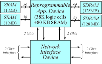
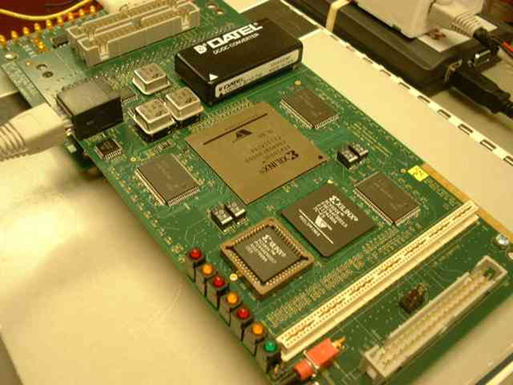
The FPX is a programmable hardware device that processes packets as they pass between the WUGS backplane and the line card. All of the logic on the FPX is implemented with two FPGA devices: the Network Interface Device (NID) and the Reprogrammable Application Device (RAD). The FPX is implemented on a 20 cm x 10.5 cm printed circuit board that interconnects the FPGAs with multiple banks of memory.
The Network Interface Device (NID) controls how packets are routed to and from its modules. It also provides mechanisms to load hardware modules over the network. These two features allow the NID to dynamically load and unload modules on the RAD without affecting the switching of other traffic flows or the processing of packets by the other modules in the system.
The NID has several components, all of which are implemented on a Xilinx Virtex XCV-600E FPGA device. It contains: 1) A four-port switch to transfer data between ports; 2) Flow look-up tables on each port to selectively route flows; 3) An on-chip Control Cell Processor to process control cells that are transmitted and received over the network; 4) Logic to reprogram the FPGA hardware on the RAD; and 5) Synchronous and asynchronous interfaces to the four network ports that surround the NID.
A key feature of the FPX is that it allows the NSP to perform packet processing functions in modular hardware components. These modules are implemented as regions of FPGA logic on the RAD. A standard interface has been developed that allows a module to process the streaming data in the packets as they flow through the module and to interface with off-chip memory. Each module on the RAD connects to one Static Random Access Memory (SRAM) and to one wide Synchronous Dynamic RAM (SDRAM). In total, the modules implemented on the RAD have full control over four independent banks of memory. The SRAM is used for applications that need to implement table look-up operations such as the routing table for the Fast IP Look-up (FIPL) module. The other modules in the system can be programmed over the network to implement user-defined functionality.
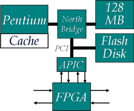
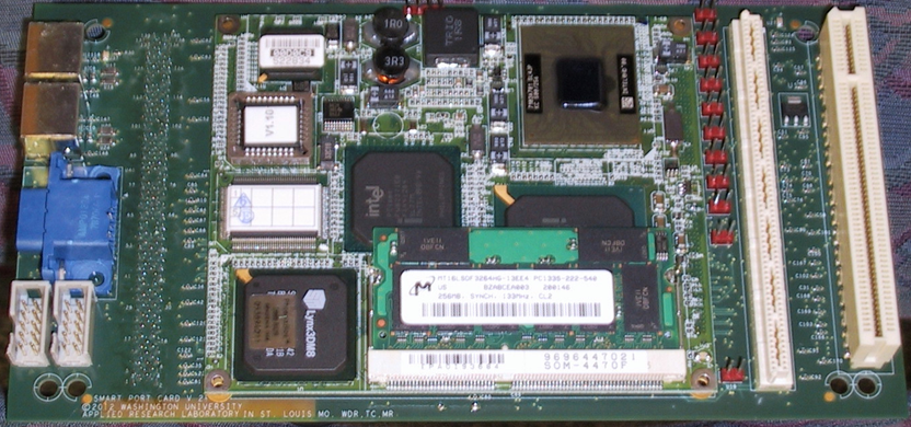
As shown in Fig. 3, the Smart Port Card (SPC) consists of an embedded Intel processor module, 64 MBytes of DRAM, an FPGA that provides south bridge functionality, and a Washington University APIC ATM host-network interface. The SPC runs a version of the NetBSD operating system that has been substantially modified to support fast packet forwarding, active network processing and network management.
The Intel embedded module contains a 500 MHz Pentium III processor, north bridge and L2 cache. The "System FPGA" provides the functionality of the south bridge chip found in a normal Pentium system and is implemented using a Xilinx XC4020XLA-08 Field Programmable Gate Array (FPGA). It contains a small boot ROM, a Programmable Interval Timer (PIT), a Programmable Interrupt Controller (PIC), a dual UART interface, and a modified Real Time Clock (RTC').
On the SPC, ATM cells are handled by the APIC. Each of the ATM ports of the APIC can be independently operated at full duplex rates ranging from 155 Mb/s to 1.2 Gb/s. The APIC supports AAL-5 and is capable of performing segmentation and reassembly at the maximum bus rate (1.05 Gb/s peak for PCI-32). The APIC directly transfers ATM frames to and from host memory and can be programmed so that cells of selected channels pass directly from one ATM port to another.
We have customized NetBSD to use a disk image stored in main memory, a serial console, a self configuring APIC device driver and a fake BIOS. The fake BIOS program acts like a boot loader: it performs some of the actions which are normally done by a Pentium BIOS and the NetBSD boot loader during power-up.
| Tutorial >> The ONL Architecture |
|